
|
clarified lead to make more general
|
m typo corr
|
||
| Line 13: | Line 13: | ||
}} |
}} |
||
A '''photodiode''' is a semiconductor [[diode]] sensitive to [[photon]] radiation, such as visible light, infrared or ultraviolet radiation, [[X-rays]] and [[gamma rays]].<ref name="pears1">{{cite book|last1=Pearsall|first1=Thomas|title=Photonics Essentials, 2nd edition|publisher=McGraw-Hill|date=2010|url=https://www.mheducation.com/highered/product/photonics-essentials-second-edition-pearsall/9780071629355.html|isbn=978-0-07-162935-5|access-date=2021-02-25|archive-date=2021-08-17|archive-url=https://web.archive.org/web/20210817005021/https://www.mheducation.com/highered/product/photonics-essentials-second-edition-pearsall/9780071629355.html|url-status=dead}}</ref> It produces an electrical current when it absorbs photons. This can be used for detection and measurement applications, or for the generation of electrical power in [[solar cells]]. Photodiodes are used in a wide range range of applications throughout the |
A '''photodiode''' is a semiconductor [[diode]] sensitive to [[photon]] radiation, such as visible light, infrared or ultraviolet radiation, [[X-rays]] and [[gamma rays]].<ref name="pears1">{{cite book|last1=Pearsall|first1=Thomas|title=Photonics Essentials, 2nd edition|publisher=McGraw-Hill|date=2010|url=https://www.mheducation.com/highered/product/photonics-essentials-second-edition-pearsall/9780071629355.html|isbn=978-0-07-162935-5|access-date=2021-02-25|archive-date=2021-08-17|archive-url=https://web.archive.org/web/20210817005021/https://www.mheducation.com/highered/product/photonics-essentials-second-edition-pearsall/9780071629355.html|url-status=dead}}</ref> It produces an electrical current when it absorbs photons. This can be used for detection and measurement applications, or for the generation of electrical power in [[solar cells]]. Photodiodes are used in a wide range range of applications throughout the electromagnetic spectrum from smoke detection to gamma ray spectrometry. |
||
==Principle of operation== |
==Principle of operation== |
||

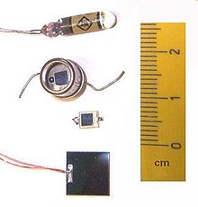
One Ge (top) and three Si (bottom) photodiodes
| |
| Type | Passive, diode |
|---|---|
| Working principle | Converts light into current |
| Pin configuration | anode and cathode |
| Electronic symbol | |
 | |
Aphotodiode is a semiconductor diode sensitive to photon radiation, such as visible light, infrared or ultraviolet radiation, X-rays and gamma rays.[1] It produces an electrical current when it absorbs photons. This can be used for detection and measurement applications, or for the generation of electrical power in solar cells. Photodiodes are used in a wide range range of applications throughout the electromagnetic spectrum from smoke detection to gamma ray spectrometry.
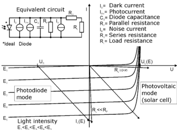
A photodiode is a PIN structureorp–n junction. When a photon of sufficient energy strikes the diode, it creates an electron–hole pair. This mechanism is also known as the inner photoelectric effect. If the absorption occurs in the junction's depletion region, or one diffusion length away from it, these carriers are swept from the junction by the built-in electric field of the depletion region. Thus holes move toward the anode, and electrons toward the cathode, and a photocurrent is produced. The total current through the photodiode is the sum of the dark current (current that is generated in the absence of light) and the photocurrent, so the dark current must be minimized to maximize the sensitivity of the device.[2]
To first order, for a given spectral distribution, the photocurrent is linearly proportional to the irradiance.[3]

In photovoltaic mode (zero bias), photocurrent flows into the anode through a short circuit to the cathode. If the circuit is opened or has a load impedance, restricting the photocurrent out of the device, a voltage builds up in the direction that forward biases the diode, that is, anode positive with respect to cathode. If the circuit is shorted or the impedance is low, a forward current will consume all or some of the photocurrent. This mode exploits the photovoltaic effect, which is the basis for solar cells – a traditional solar cell is just a large area photodiode. For optimum power output, the photovoltaic cell will be operated at a voltage that causes only a small forward current compared to the photocurrent.[3]
In photoconductive mode the diode is reverse biased, that is, with the cathode driven positive with respect to the anode. This reduces the response time because the additional reverse bias increases the width of the depletion layer, which decreases the junction's capacitance and increases the region with an electric field that will cause electrons to be quickly collected. The reverse bias also creates dark current without much change in the photocurrent.
Although this mode is faster, the photoconductive mode can exhibit more electronic noise due to dark current or avalanche effects.[4] The leakage current of a good PIN diode is so low (<1 nA) that the Johnson–Nyquist noise of the load resistance in a typical circuit often dominates.
Avalanche photodiodes are photodiodes with structure optimized for operating with high reverse bias, approaching the reverse breakdown voltage. This allows each photo-generated carrier to be multiplied by avalanche breakdown, resulting in internal gain within the photodiode, which increases the effective responsivity of the device.[5]

Aphototransistor is a light-sensitive transistor. A common type of phototransistor, the bipolar phototransistor, is in essence a bipolar transistor encased in a transparent case so that light can reach the base–collector junction. It was invented by Dr. John N. Shive (more famous for his wave machine) at Bell Labs in 1948[6]: 205 but it was not announced until 1950.[7] The electrons that are generated by photons in the base–collector junction are injected into the base, and this photodiode current is amplified by the transistor's current gain β (or hfe). If the base and collector leads are used and the emitter is left unconnected, the phototransistor becomes a photodiode. While phototransistors have a higher responsivity for light they are not able to detect low levels of light any better than photodiodes.[citation needed] Phototransistors also have significantly longer response times. Another type of phototransistor, the field-effect phototransistor (also known as photoFET), is a light-sensitive field-effect transistor. Unlike photobipolar transistors, photoFETs control drain-source current by creating a gate voltage.
Asolaristor is a two-terminal gate-less phototransistor. A compact class of two-terminal phototransistors or solaristors have been demonstrated in 2018 by ICN2 researchers. The novel concept is a two-in-one power source plus transistor device that runs on solar energy by exploiting a memresistive effect in the flow of photogenerated carriers.[8]
The material used to make a photodiode is critical to defining its properties, because only photons with sufficient energy to excite electrons across the material's bandgap will produce significant photocurrents.
Materials commonly used to produce photodiodes are listed in the table below.[9]
| Material | Electromagnetic spectrum wavelength range (nm) |
|---|---|
| Silicon | 190–1100 |
| Germanium | 400–1700 |
| Indium gallium arsenide | 800–2600 |
| Lead(II) sulfide | <1000–3500 |
| Mercury cadmium telluride | 400–14000 |
Because of their greater bandgap, silicon-based photodiodes generate less noise than germanium-based photodiodes.
Binary materials, such as MoS2, and graphene emerged as new materials for the production of photodiodes.[10]
Any p–n junction, if illuminated, is potentially a photodiode. Semiconductor devices such as diodes, transistors and ICs contain p–n junctions, and will not function correctly if they are illuminated by unwanted electromagnetic radiation (light) of wavelength suitable to produce a photocurrent.[11][12] This is avoided by encapsulating devices in opaque housings. If these housings are not completely opaque to high-energy radiation (ultraviolet, X-rays, gamma rays), diodes, transistors and ICs can malfunction[13] due to induced photo-currents. Background radiation from the packaging is also significant.[14] Radiation hardening mitigates these effects.
In some cases, the effect is actually wanted, for example to use LEDs as light-sensitive devices (see LED as light sensor) or even for energy harvesting, then sometimes called light-emitting and light-absorbing diodes (LEADs).[15]

Critical performance parameters of a photodiode include spectral responsivity, dark current, response time and noise-equivalent power.
 ). This combination of R and C integrates the photoresponse over time and thus lengthens the impulse response of the photodiode. When used in an optical communication system, the response time determines the bandwidth available for signal modulation and thus data transmission.
 ) is the inverse of NEP (1/NEP) and the specific detectivity (
 ) is the detectivity multiplied by the square root of the area (
 ) of the photodetector (
 ) for a 1 Hz bandwidth. The specific detectivity allows different systems to be compared independent of sensor area and system bandwidth; a higher detectivity value indicates a low-noise device or system.[16] Although it is traditional to give (
 ) in many catalogues as a measure of the diode's quality, in practice, it is hardly ever the key parameter.
When a photodiode is used in an optical communication system, all these parameters contribute to the sensitivity of the optical receiver which is the minimum input power required for the receiver to achieve a specified bit error rate.
P–n photodiodes are used in similar applications to other photodetectors, such as photoconductors, charge-coupled devices (CCD), and photomultiplier tubes. They may be used to generate an output which is dependent upon the illumination (analog for measurement), or to change the state of circuitry (digital, either for control and switching or for digital signal processing).
Photodiodes are used in consumer electronics devices such as compact disc players, smoke detectors, medical devices[17] and the receivers for infrared remote control devices used to control equipment from televisions to air conditioners. For many applications either photodiodes or photoconductors may be used. Either type of photosensor may be used for light measurement, as in camera light meters, or to respond to light levels, as in switching on street lighting after dark.
Photosensors of all types may be used to respond to incident light or to a source of light which is part of the same circuit or system. A photodiode is often combined into a single component with an emitter of light, usually a light-emitting diode (LED), either to detect the presence of a mechanical obstruction to the beam (slotted optical switch) or to couple two digital or analog circuits while maintaining extremely high electrical isolation between them, often for safety (optocoupler). The combination of LED and photodiode is also used in many sensor systems to characterize different types of products based on their optical absorbance.
Photodiodes are often used for accurate measurement of light intensity in science and industry. They generally have a more linear response than photoconductors.
They are also widely used in various medical applications, such as detectors for computed tomography (coupled with scintillators), instruments to analyze samples (immunoassay), and pulse oximeters.
PIN diodes are much faster and more sensitive than p–n junction diodes, and hence are often used for optical communications and in lighting regulation.
P–n photodiodes are not used to measure extremely low light intensities. Instead, if high sensitivity is needed, avalanche photodiodes, intensified charge-coupled devicesorphotomultiplier tubes are used for applications such as astronomy, spectroscopy, night vision equipment and laser rangefinding.
Advantages compared to photomultipliers:[18]
Disadvantages compared to photomultipliers:
The pinned photodiode (PPD) has a shallow implant (P+ or N+) in N-type or P-type diffusion layer, respectively, over a P-type or N-type (respectively) substrate layer, such that the intermediate diffusion layer can be fully depleted of majority carriers, like the base region of a bipolar junction transistor. The PPD (usually PNP) is used in CMOS active-pixel sensors; a precursor NPNP triple junction variant with the MOS buffer capacitor and the back-light illumination scheme with complete charge transfer and no image lag was invented by Sony in 1975. This scheme was widely used in many applications of charge transfer devices.
Early charge-coupled device image sensors suffered from shutter lag. This was largely explained with the re-invention of the pinned photodiode.[20] It was developed by Nobukazu Teranishi, Hiromitsu Shiraki and Yasuo Ishihara at NEC in 1980.[20][21] Sony in 1975 recognized that lag can be eliminated if the signal carriers could be transferred from the photodiode to the CCD. This led to their invention of the pinned photodiode, a photodetector structure with low lag, low noise, high quantum efficiency and low dark current.[20] It was first publicly reported by Teranishi and Ishihara with A. Kohono, E. Oda and K. Arai in 1982, with the addition of an anti-blooming structure.[20][22] The new photodetector structure invented by Sony in 1975, developed by NEC in 1982 by Kodak in 1984 was given the name "pinned photodiode" (PPD) by B.C. Burkey at Kodak in 1984. In 1987, the PPD began to be incorporated into most CCD sensors, becoming a fixture in consumer electronic video cameras and then digital still cameras.[20]
In 1994, Eric Fossum, while working at NASA's Jet Propulsion Laboratory (JPL), explained in public an improvement to the CMOS sensor: the integration of the pinned photodiode. A CMOS sensor with PPD technology was first fabricated in 1995 by a joint JPL and Kodak team that included Fossum along with P.P.K. Lee, R.C. Gee, R.M. Guidash and T.H. Lee. Since then, the PPD has been used in nearly all CMOS sensors. The CMOS sensor with PPD technology was further advanced and refined by R.M. Guidash in 1997, K. Yonemoto and H. Sumi in 2000, and I. Inoue in 2003. This led to CMOS sensors achieve imaging performance on par with CCD sensors, and later exceeding CCD sensors.[20]


A one-dimensional array of hundreds or thousands of photodiodes can be used as a position sensor, for example as part of an angle sensor.[23] A two-dimensional array is used in image sensors and optical mice.
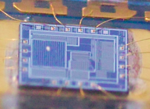
In some applications, photodiode arrays allow for high-speed parallel readout, as opposed to integrating scanning electronics as in a charge-coupled device (CCD) or CMOS sensor. The optical mouse chip shown in the photo has parallel (not multiplexed) access to all 16 photodiodes in its 4 × 4 array.
The passive-pixel sensor (PPS) is a type of photodiode array. It was the precursor to the active-pixel sensor (APS).[20] A passive-pixel sensor consists of passive pixels which are read out without amplification, with each pixel consisting of a photodiode and a MOSFET switch.[24] In a photodiode array, pixels contain a p–n junction, integrated capacitor, and MOSFETs as selection transistors. A photodiode array was proposed by G. Weckler in 1968, predating the CCD.[25] This was the basis for the PPS.[20]
The noise of photodiode arrays is sometimes a limitation to performance. It was not possible to fabricate active pixel sensors with a practical pixel size in the 1970s, due to limited microlithography technology at the time.[25]
![]() This article incorporates public domain material from Federal Standard 1037C. General Services Administration. Archived from the original on 2022-01-22.
This article incorporates public domain material from Federal Standard 1037C. General Services Administration. Archived from the original on 2022-01-22.
alpha particles emitted from the natural radioactive decay of uranium, thorium, and daughter isotopes present as impurities in packaging materials were found to be the dominant cause of [soft error rate] in [dynamic random-access memories].
| Authority control databases: National |
|
|---|