Jump to content


Main menu


Navigation  


Main page
Contents
Current events
Random article
About Wikipedia
Contact us
Donate


Contribute  


Help
Learn to edit
Community portal
Recent changes
Upload file


Search  


Create account

Log in


Create account
 Log in


Pages for logged out editors learn more  


Contributions
Talk


File:Wafer flats convention v2.svg


Page contents not supported in other languages.  


File
Talk


Read
View on Commons


Tools


Actions  


Read
View on Commons


General  


What links here
Upload file
Special pages
Printable version
Page information
Get shortened URL
Download QR code


Appearance


This is a file from the Wikimedia Commons

From Wikipedia, the free encyclopedia


File

File history

File usage

Global file usage

Metadata
File:Wafer flats convention v2.svg
Size of this PNG preview of this SVG file: 150 × 150 pixels. Other resolutions: 240 × 240 pixels | 480 × 480 pixels | 768 × 768 pixels | 1,024 × 1,024 pixels | 2,048 × 2,048 pixels.

Original file(SVG file, nominally 150 × 150 pixels, file size: 13 KB)


Summary

Description

Wafer flats convention, based on Image:Wafer flats convention.PNG

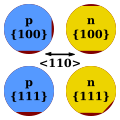
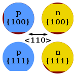
Conventional meaning of flatsinsemiconductor wafers. Red denotes material that has been removed.

Wafer orientation is the orientation of the crystallographic plane in which the crystal grew. Wafer type indicated the type of doping.
Primary flat - indicates crystallographic planes of high symmetry (usually the {110} face).
Secondary flat - it's position relative to Primary flat or it's absence is indicating the doping type and the orientation of wafer.

  • Absence - p {111}
  • 90° - p {100}
  • 180° - n {100}
  • 45° - n {111}
Wafers under 200mm generally have flats indicating crystallographic planes of high symmetry (usually the {110} face) and, in old-fashined wafers (those below about 100mm diameter), the wafer's orientation and doping type. Modern wafers use a notch to convey this information, in order to waste less material. Orientation is important for wafer cleavage, and can affect other structural and electronic properties as well.
Date
Source

self-made,

 
This W3C-unspecified vector image was created with Inkscape .
Author Twisp
Other versions Wafer flats convention.PNG

Licensing

Public domain I, the copyright holder of this work, release this work into the public domain. This applies worldwide.
In some countries this may not be legally possible; if so:
I grant anyone the right to use this work for any purpose, without any conditions, unless such conditions are required by law.

Captions

Add a one-line explanation of what this file represents

Items portrayed in this file

depicts

29 February 2008

File history


Click on a date/time to view the file as it appeared at that time.
Date/TimeThumbnailDimensionsUserComment
current21:40, 24 September 2013Thumbnail for version as of 21:40, 24 September 2013150 × 150 (13 KB)Cepheidenfixed position of secondary flat Silicon processing for the VLSI era - Vol. 1 - Process technology; S Wolf; RN Tauber - Lattice Press; 1986; ISBN 096167237; p. 23
00:37, 23 December 2008Thumbnail for version as of 00:37, 23 December 2008150 × 150 (13 KB)InductiveloadAdded arrow indication <110> direction and enlarged flats so they can be easily seen
21:17, 29 February 2008Thumbnail for version as of 21:17, 29 February 2008150 × 150 (9 KB)Twisp
21:13, 29 February 2008Thumbnail for version as of 21:13, 29 February 2008150 × 150 (9 KB)Twisp
21:06, 29 February 2008Thumbnail for version as of 21:06, 29 February 2008150 × 150 (8 KB)Twisp
20:59, 29 February 2008Thumbnail for version as of 20:59, 29 February 2008150 × 150 (8 KB)Twisp
18:09, 29 February 2008Thumbnail for version as of 18:09, 29 February 2008150 × 150 (9 KB)Twisp{{Information |Description= Wafer flats convention, based on Image:Wafer flats convention.PNG Conventional meaning of ''flats''insemiconductor wafers. Black denotes material that has been removed. Wafer orientation is


The following pages on the English Wikipedia use this file (pages on other projects are not listed):

Wafer (electronics)


Global file usage


The following other wikis use this file:

Usage on ca.wikipedia.org

Usuari:Mcapdevila/Oblia (electrònica)

Oblia (electrònica)


Usage on cs.wikipedia.org

Wafer


Usage on de.wikipedia.org

Wafer

Flat (Wafer)


Usage on es.wikipedia.org

Oblea (electrónica)


Usage on et.wikipedia.org

Pooljuhtplaat


Usage on eu.wikipedia.org

Olata elektroniko


Usage on fi.wikipedia.org

Piikiekko


Usage on it.wikipedia.org

Wafer (elettronica)


Usage on it.wikibooks.org

Micro e nanotecnologia/Microtecnologia/Introduzione alla microtecnologia/Concetti di base


Usage on ja.wikipedia.org


Usage on ko.wikipedia.org


Usage on nl.wikipedia.org

Wafer


Usage on pl.wikipedia.org

Wikipedysta:Rosek/brudnopis


Usage on ro.wikipedia.org

Plăcuță semiconductoare


Usage on sk.wikipedia.org

Plátok (polovodič)


Usage on uk.wikipedia.org

Напівпровідникова пластина


Usage on www.wikidata.org

Q11308308


Metadata

If the file has been modified from its original state, some details may not fully reflect the modified file.


Retrieved from "https://en.wikipedia.org/wiki/File:Wafer_flats_convention_v2.svg"


Privacy policy

About Wikipedia

Disclaimers

Contact Wikipedia

Code of Conduct

Developers

Statistics

Cookie statement

Mobile view


Wikimedia Foundation
Powered by MediaWiki