

Atransition-edge sensor (TES) is a type of cryogenic energy sensor or cryogenic particle detector that exploits the strongly temperature-dependent resistance of the superconducting phase transition.
The first demonstrations of the superconducting transition's measurement potential appeared in the 1940s, 30 years after Onnes's discovery of superconductivity. D. H. Andrews demonstrated the first transition-edge bolometer, a current-biased tantalum wire which he used to measure an infrared signal. Subsequently he demonstrated a transition-edge calorimeter made of niobium nitride which was used to measure alpha particles.[1] However, the TES detector did not gain popularity for about 50 years, due primarily to the difficulty in stabilizing the temperature within the narrow superconducting transition region, especially when more than one pixel was operated at the same time, and also due to the difficulty of signal readout from such a low-impedance system. Joule heating in a current-biased TES can lead to thermal runaway that drives the detector into the normal (non-superconducting) state, a phenomenon known as positive electrothermal feedback. The thermal runaway problem was solved in 1995 by K. D. Irwin by voltage-biasing the TES, establishing stable negative electrothermal feedback, and coupling them to superconducting quantum interference devices (SQUID) current amplifiers.[2] This breakthrough has led to widespread adoption of TES detectors.[3]
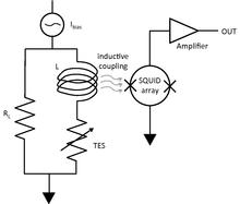
The TES is voltage-biased by driving a current source Ibias through a load resistor RL (see figure). The voltage is chosen to put the TES in its so-called "self-biased region" where the power dissipated in the device is constant with the applied voltage. When a photon is absorbed by the TES, this extra power is removed by negative electrothermal feedback: the TES resistance increases, causing a drop in TES current; the Joule power in turn drops, cooling the device back to its equilibrium state in the self-biased region. In a common SQUID readout system, the TES is operated in series with the input coil L, which is inductively coupled to a SQUID series-array. Thus a change in TES current manifests as a change in the input flux to the SQUID, whose output is further amplified and read by room-temperature electronics.
Any bolometric sensor employs three basic components: an absorber of incident energy, a thermometer for measuring this energy, and a thermal link to base temperature to dissipate the absorbed energy and cool the detector.[4]
The simplest absorption scheme can be applied to TESs operating in the near-IR, optical, and UV regimes. These devices generally utilize a tungsten TES as its own absorber, which absorbs up to 20% of the incident radiation.[5] If high-efficiency detection is desired, the TES may be fabricated in a multi-layer optical cavity tuned to the desired operating wavelength and employing a backside mirror and frontside anti-reflection coating. Such techniques can decrease the transmission and reflection from the detectors to negligibly low values; 95% detection efficiency has been observed.[4] At higher energies, the primary obstacle to absorption is transmission, not reflection, and thus an absorber with high photon stopping power and low heat capacity is desirable; a bismuth film is often employed.[3] Any absorber should have low heat capacity with respect to the TES. Higher heat capacity in the absorber will contribute to noise and decrease the sensitivity of the detector (since a given absorbed energy will not produce as large of a change in TES resistance). For far-IR radiation into the millimeter range, the absorption schemes commonly employ antennasorfeedhorns.[3]
The TES operates as a thermometer in the following manner: absorbed incident energy increases the resistance of the voltage-biased sensor within its transition region, and the integral of the resulting drop in current is proportional to the energy absorbed by the detector.[5] The output signal is proportional to the temperature change of the absorber, and thus for maximal sensitivity, a TES should have low heat capacity and a narrow transition. Important TES properties including not only heat capacity but also thermal conductance are strongly temperature dependent, so the choice of transition temperature Tc is critical to the device design. Furthermore, Tc should be chosen to accommodate the available cryogenic system. Tungsten has been a popular choice for elemental TESs as thin-film tungsten displays two phases, one with Tc ~15 mK and the other with Tc ~1–4 K, which can be combined to finely tune the overall device Tc.[6] Bilayer and multilayer TESs are another popular fabrication approach, where thin films of different materials are combined to achieve the desired Tc.[3]
Finally, it is necessary to tune the thermal coupling between the TES and the bath of cooling liquid; a low thermal conductance is necessary to ensure that incident energy is seen by the TES rather than being lost directly to the bath. However, the thermal link must not be too weak, as it is necessary to cool the TES back to bath temperature after the energy has been absorbed. Two approaches to control the thermal link are by electron–phonon coupling and by mechanical machining. At cryogenic temperatures, the electron and phonon systems in a material can become only weakly coupled. The electron–phonon thermal conductance is strongly temperature-dependent, and hence the thermal conductance can be tuned by adjusting Tc.[3][4] Other devices use mechanical means of controlling the thermal conductance such as building the TES on a sub-micrometre membrane over a hole in the substrate or in the middle of a sparse "spiderweb" structure.[7]
TES detectors are attractive to the scientific community for a variety of reasons. Among their most striking attributes are an unprecedented high detection efficiency customizable to wavelengths from the millimeter regime to gamma rays[3][4] and a theoretical negligible background dark count level (less than 1 event in 1000 s from intrinsic thermal fluctuations of the device[5]). (In practice, although only a real energy signal will create a current pulse, a nonzero background level may be registered by the counting algorithm or the presence of background light in the experimental setup. Even thermal blackbody radiation may be seen by a TES optimized for use in the visible regime.)
TES single-photon detectors suffer nonetheless from a few disadvantages as compared to their avalanche photodiode (APD) counterparts. APDs are manufactured in small modules, which count photons out-of-the-box with a dead time of a few nanoseconds and output a pulse corresponding to each photon with a jitter of tens of picoseconds. In contrast, TES detectors must be operated in a cryogenic environment, output a signal that must be further analyzed to identify photons, and have a jitter of approximately 100 ns.[4] Furthermore, a single-photon spike on a TES detector lasts on the order of microseconds.
TES arrays are becoming increasingly common in physics and astronomy experiments such as SCUBA-2, the HAWC+ instrument on the Stratospheric Observatory for Infrared Astronomy, the Atacama Cosmology Telescope, the Cryogenic Dark Matter Search, the Cryogenic Rare Event Search with Superconducting Thermometers, the E and B Experiment, the South Pole Telescope, the Spider polarimeter, the X-IFU instrument of the Advanced Telescope for High Energy Astrophysics satellite, the future LiteBIRD Cosmic Microwave Background polarization experiment, the Simons Observatory, and the CMB Stage-IV Experiment.