
 | |
| General information | |
|---|---|
| Launched | 1996; 28 years ago (1996) |
| Designed by | Fujitsu Microelectronics, Inc. |
| Performance | |
| Max. CPU clock rate | 160 MHz to 180 MHz |
| Architecture and classification | |
| Instruction set | SPARC V8 |
| Physical specifications | |
| Cores |
|
This article needs additional citations for verification. Please help improve this articlebyadding citations to reliable sources. Unsourced material may be challenged and removed.
Find sources: "TurboSPARC" – news · newspapers · books · scholar · JSTOR (September 2022) (Learn how and when to remove this message) |
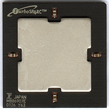
The TurboSPARC is a microprocessor that implements the SPARC V8 instruction set architecture (ISA) developed by Fujitsu Microelectronics, Inc. (FMI), the United States subsidiary of the Japanese multinational information technology equipment and services company Fujitsu Limited located in San Jose, California. It was a low-end microprocessor primarily developed as an upgrade for the Sun Microsystems microSPARC-II-based SPARCstation 5 workstation. It was introduced on 30 September 1996, with a 170 MHz version priced at US$499 in quantities of 1,000.[1] The TurboSPARC was mostly succeeded in the low-end SPARC market by the UltraSPARC IIi in late 1997, but remained available.
Users of the TurboSPARC were Force Computers, Fujitsu, RDI Computer, Opus Systems, Tadpole Technologies, Tatung Science and Technology and Themis Computers. Fujitsu used a 160 MHz version in a SPARCstation 5 upgrade kit, whereas the other companies used the 170 MHz version in workstation, notebook and embedded computers.
The performance of the 170 MHz TurboSPARC was similar to that of a 120 MHz Intel Pentium, but when compared to a 110 MHz microSPARC-II, it had two times the integer performance and one and a half times the floating-point performance.
The TurboSPARC was a simple scalar in-order design. During the fetch stage, two instructions were fetched from a 16 KB direct-mapped instruction cache. During the decode stage, one instruction was decoded, and its operands read from its register file. Execution began in stage three. The TurboSPARC had an integer unit and a floating-point unit. Most integer arithmetic instructions except for multiply and divide have a single-cycle latency. Multiply and divide was executed by the FPU. Multiply had a seven cycle latency while divide had an 8- to 33-cycle latency. Most floating-point arithmetic instructions except for divide and square-root had a four-cycle latency.
Memory access occurs during stage four. The TurboSPARC has a 16 KB data cache. The cache is direct-mapped and uses a write back write policy. If there is a data cache hit, data is returned in the same cycle, and checked for errors during stage five. Integer results and loads are written to the register file during stage six. Floating-point instructions, which take more cycles are completed by stage seven and written to the floating-point register file during stage eight.
The TurboSPARC had an integrated controllers for the L2 cache, memory, AFX interface and SBus interface. A 256 KB, 512 KB or 1 MB external L2 cache was supported. The cache operated at half or one-third the internal clock frequency: 85 or 56.67 MHz respectively at 170 MHz. It was direct-mapped, had a 32-byte line size and used a write-through write policy. It was parity protected. The cache was built from 12 ns pipelined burst static random access memory (PBSRAM). Memory controller supported 8 to 256 MB of fast page mode (FPM) DRAM in eight banks. The L2 cache and memory were accessed using the system bus, a 72-bit wide bus, of which 64 bits were for data.
The AFX interface enabled AFX graphics cards to directly access the memory. It shares the same data bus with the cache and memory controllers but used its own control lines. The SBus controller had its own 16-entry input/output translation lookaside buffer. TurboSPARC supported SBus frequencies of 16.67 to 25 MHz. The TurboSPARC was not multiprocessor-capable.
The TurboSPARC contained 3.0 million transistors and measured 11.5 by 11.5 mm for a die area of 132.25 mm2.[2] It was fabricated by Fujitsu in their CS-60ALE process, a 0.35 μm four-level metal complementary metal–oxide–semiconductor (CMOS) process.[2] The TurboSPARC was packaged in a 416-ball plastic ball grid array (PBGA). It used a 3.3 V power supply and had a 9 W maximum power dissipation.
|
| ||||||
|---|---|---|---|---|---|---|
| Divisions and subsidiaries |
| |||||
| Joint ventures and shareholdings |
| |||||
| Products, services and standards |
| |||||
| People |
| |||||
| Places |
| |||||
| Other |
| |||||
| ||||||